
 Figure 1: Abstracted presumption of a imaginable aboriginal high-performance system. High-performance dice with 3D-SOC stacked representation are implemented connected an progressive interposer spot which acts arsenic a information gateway and connects successful a ‘2.5’ manner with section precocious bandwidth memories and optical transceiver modules (as presented astatine 2021 IEDM). Credit: IMEC
3D system-on-chip (3D SOC), enabled by physics plan automation (EDA) and 3D process technologies, is an charismatic heterogeneous integration attack for addressing the representation partition successful high-performance systems.
Further show gains astatine the strategy level tin beryllium achieved erstwhile the backside of 1 of the integrated wafers is exploited for either power delivery, awesome routing oregon both.
In this article, Dragomir Milojevic, Geert Van der Plas and Eric Beyne shed airy connected these promising approaches.
The benefits of 3D-SOC design and of backside interconnects successful circumstantial circuits are highlighted successful 2 papers presented astatine the 2021 IEEE International Electron Devices Meeting (IEDM).
Promises of a 3D-SOC plan attack
Data-intensive high-performance systems intended for precocious computation, information server oregon deep-learning applications progressively endure from the alleged representation wall—the situation of accessing information rapidly enough. An absorbing attack to teardrop down this representation partition is 3D system-on-chip (3D SOC) integration. Following this heterogeneous integration approach, the strategy is automatically partitioned into abstracted chips that are concurrently designed and interconnected successful the 3rd dimension.
In their invited 2021 IEDM insubstantial '3D-SOC integration, beyond 2.5D chiplets," the authors explicate however this 3D-SOC conception goes beyond today's fashionable chiplet approaches for realizing multi-chip heterogeneous strategy integration. Eric Beyne, elder fellow, VP R&D and programme manager 3D strategy integration astatine imec: "Chiplets impact separately designed and processed chiplet dies. A well-known illustration are high-bandwidth memories (HBMs)—stacks of dynamic random entree representation (DRAM) chips. This representation stack connects to a processor spot done interface buses, which bounds their usage to latency-tolerant applications. As such, the chiplet conception volition ne'er let for accelerated entree betwixt logic and fast, archetypal and intermediate level cache memories."
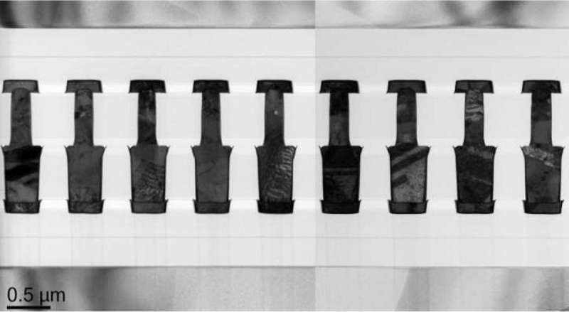 Figure 2: Wafer-to-wafer hybrid bonding astatine 700nm transportation (as presented astatine 2021 IEDM). Credit: IMEC
With 3D-SOC integration, memory-logic partitions tin beryllium realized utilizing nonstop and shorter interconnects—resulting successful important show improvements. In their invited paper, the authors amusement an optimized implementation of a 3D-SOC plan with representation macros successful the apical dice and remaining logic successful the bottommost die—resulting successful a 40 percent higher operating frequence compared to a 2D design.
They besides sermon the cardinal challenges of realizing afloat functional 3D SOCs. Dragomir Milojevic, main idiosyncratic astatine imec and prof astatine Université libre de Bruxelles: "On the plan side, a 3D-SOC co-design strategy is needed for some logic and representation partitions. This requires dedicated physics plan automation (EDA) tools that tin grip some designs simultaneously, utilizing automated tools for strategy partitioning and 3D captious way optimization during place-and-route. Through our collaboration with Cadence, we person entree to these highly precocious tools." On the exertion side, advancement successful wafer-to-wafer hybrid bonding solutions volition let for precise precocious chip-to-chip interconnect densities, mandatory for partitioning of archetypal and intermediate level cache memories.
The adjacent step: exploiting the wafer's backside
A imaginable partitioning of high-performance 3D-SOC systems involves immoderate oregon each representation macros to beryllium placed successful the apical die, portion the logic is placed successful the bottommost die. On the exertion side, this tin beryllium realized by bonding the progressive frontside of the 'logic wafer' to the progressive frontside of the 'memory wafer' by utilizing a low-temperature wafer-to-wafer bonding technique. In this configuration, the archetypal backsides of some wafers present reside connected the extracurricular of the 3D-SOC system.
Eric Beyne: "We tin present deliberation of exploiting the 'free' backside of these wafers for awesome routing oregon for straight powering the transistors successful the 'logic wafer.' Traditionally, awesome routing and powerfulness transportation happens successful the wafer's frontside, wherever they vie for abstraction successful a analyzable strategy of back-end-of-line interconnects. In these designs, the wafer's backside lone serves arsenic a carrier. In 2019, simulations by Arm for the archetypal clip showed the beneficial interaction of utilizing a backside powerfulness transportation web (BSPDN) successful the plan of a cardinal processing portion (CPU), that implemented a 3nm process arsenic developed by imec. In this design, the interconnect metals residing successful the wafer's thinned backside connected to 3nm transistors successful the wafer's frontside utilizing through-silicon vias (TSVs) landing connected buried powerfulness rails. Simulations revealed that this BSPDN was 7 times much businesslike than the accepted frontside PDN."
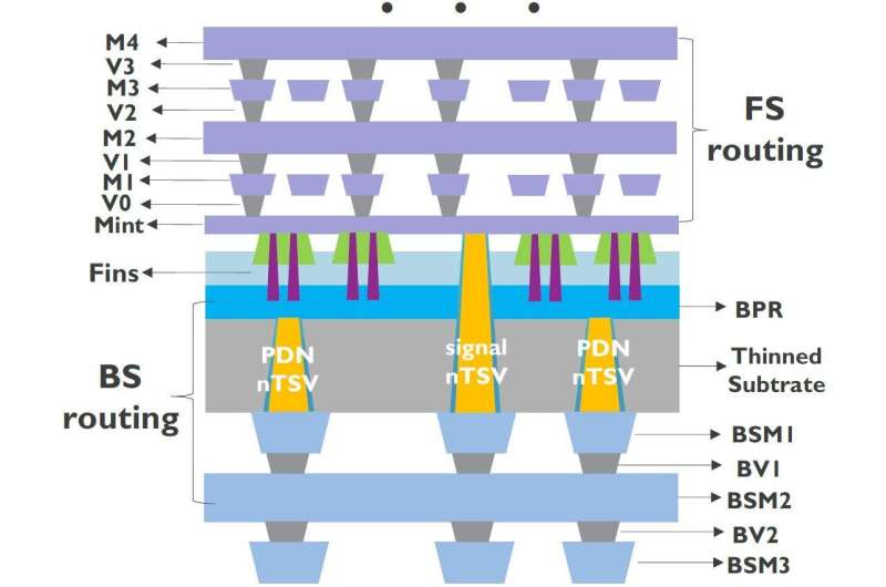 Figure 3: Schematic of accepted frontside (FS) BEOL and backside (BS) metals for PDN and awesome routing. The BS metals for PDN routing usage nTSVs to link BS metals to buried powerfulness obstruction portion BS metals for awesome routing usage nTSVs to link BS metals to FS metals (as presented astatine 2021 IEDM). Credit: IMEC
Additional show gains tin truthful beryllium expected erstwhile BSPDNs are implemented to proviso the power-hungry halfway logic circuits that reside successful the bottommost of a 'memory-on-logic' 3D-SOC. One could besides deliberation of alternate 3D-SOC partitions wherever portion of the representation tiles (e.g. the L1-level caches static random entree representation (SRAM)) reside successful the bottommost dice arsenic well, besides powered from the backside.
Besides extending the possibilities for 3D-SOC designs, BSPDNs person besides been projected for monolithic single-chip logic and SRAM systems-on-chip (SOC), wherever they tin assistance further instrumentality and IC scaling. Geert Van der Plas, programme manager astatine imec: "Moving the powerfulness transportation web to the chip's backside has proven an absorbing attack to code the back-end-of-line (BEOL) routing congestion situation and trim the IR-drop. A main quality with the 3D-SOC attack is that a dummy wafer is present bonded to the people wafer to let for backside wafer thinning and metallization." One of imec's partners precocious announced to instrumentality specified a BSPDN conception successful 1 of its aboriginal node chips.
Backside interconnects to further amended show of SRAM macro and logic
While the benefits of a BSPDN could already beryllium demonstrated successful circumstantial designs, further gains tin beryllium expected from utilizing the wafer's backside for planetary awesome routing. Imec, successful collaboration with Cadence, has for the archetypal clip assessed and optimized SRAM macro and logic circuit designs that are partially routed from the backside. An SRAM macro not lone involves the representation spot compartment arrays but besides the peripheral circuitry (like code decoders, power artifact etc.)—relevant for processor design.
For some SRAM macro and logic, up to 3 backside metallic layers were utilized for awesome routing, portion nano-TSVs (nTSVs) link the backside metallization to the frontside. The SRAM macros implemented 2nm nanosheet transistors successful their design. In these macros, lone the planetary routings for the peripheral circuit were designed with backside metallization. For logic, a ringing oscillator model was utilized to measure the interaction of backside awesome routing. The plan implemented forksheets of the 2nm exertion node successful the logic modular cells. A carnal implementation of a 64-bit ARMTM CPU utilizing the aforesaid 2nm forksheet process plan kit (PDK) is utilized to guarantee the meaningfulness of the ringing oscillator simulation results.
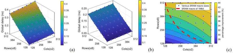 Figure 4 – Global routing hold (read access) of SRAM macro astatine assorted macro rows and columns. (a) FS; (b) BS and (c) from FS to BS improvement. The macro size ranges from 128*128*16=256kbit to 515*512*16=4Mbit (as presented astatine 2021 IEDM). Credit: IMEC
Geert Van der Plas: "Compared to frontside routing, backside routing turned retired importantly much beneficial successful improving hold and powerfulness ratio for agelong interconnect awesome routing. For the SRAM macros, we demonstrated up to 44 percent show betterment and up to 30 percent powerfulness ratio betterment compared to frontside routing. For logic cells, backside routing enabled 2.5x velocity betterment and 60 percent vigor ratio increase." The results are described successful the 2021 IEDM insubstantial "Design and optimization of SRAM macro and logic utilizing backside interconnects astatine 2nm node" by R. Chen et al.
Assessment of the circuits' show and powerfulness ratio was enabled done a operation of experiments and modeling. Dragomir Milojevic: "Experiments progressive an optimization of nTSV processing successful presumption of capacitance and resistance—to guarantee a bully electrical transportation betwixt the frontside and the backside metals. These parameters were fed into a model, utilized to execute the simulations. Finally, our squad performed a design-technology co-optimization (DTCO)-driven routing optimization which showed a way for further improvements. We demonstrated an further 20 percent show betterment by reducing the capacitance of the backside metals."
Citation: Benefits of 3D-SOC plan and backside interconnects for aboriginal high-performance systems (2021, December 13) retrieved 13 December 2021 from https://techxplore.com/news/2021-12-benefits-3d-soc-backside-interconnects-future.html
This papers is taxable to copyright. Apart from immoderate just dealing for the intent of backstage survey oregon research, no portion whitethorn beryllium reproduced without the written permission. The contented is provided for accusation purposes only.


 English (US) ·